Sunday, November 30, 2014

Avoid the use of MTBF

The use of MTBF (Mean Time Between Failures) is almost always applied wrong. As a producer of a product you would want the product to last beyond the warranty period and long enough to be perceived by the customer as a 'Quality' product. One way of quantifying this is that a product will have X% reliability at Y years with C% confidence.

MTBF is the inverse of the failure rate, NOT the life-time of the product. As example a product or assembly might have a MTBF of 400,000 device-hrs. This does not mean the product life is 400,000hrs (45.6 years)! It means the failure rate is 2.5 per million hours.

 Implicit in the concept of MTBF or it's inverse failure rate is the that the failure rate is constant. Think of the MTBF as meaning that in any given hour the possibility of failure is 1/MTBF. This is applicable during the flat portion of the 'Bath Tub' curve showing failure rate versus time (see figure). Quite often in a product there will be components that have a very low failure rate but have a wear out function that forms the right-hand side of the Bath Tub curve. For example, the product with a 400,000 device-hr MTBF might have a element that wears out at 20,000hrs as example.

One way of analyzing a product is to add up all the failure rates of the individual components. Commonly expressed as failures per billion hours this is referred to as the FIT rate (Failures in Time). For our example a product with a MTBF of 400,000 has a FIT rate of 2500.

Back to our example, a product with an MTBF of 400,000 that is operated 24/7 will have a failure rate of about (1 - exp(-t/MTBF)) in a year, or 2.2% annual failre rate (AFR). Because of the uniform distribution of failures a small sample of the failure rate may result in measured values ranging from 1% to 5%, but over a large population will be 2.2%. In 5 years this would be over 10% failures, or less than 90% reliability. In this light the MTBF of 400,000 no longer seems so good.


When designing a product from the start there should be a reliability target and a pro-forma reliability budget based on the target design. If the reliability target looks like it cannot be met then the architecture of the system needs to be re-thought out or the reliability target changed, understanding the business consequences.

Sunday, February 16, 2014

EMI Reduction of Laser Modulation

The topic discussed here involves the solution of an EMI problem caused by modulating a laser at 40Mhz. In EMI testing there were failures at multiple harmonics of the 40Mhz. The root of the problem is that the laser is a two terminal device and the case is electrically tied to the anode. A simplified LTspice circuit model of the laser driver is shown in Figure 1 showing the stray capacitance.

Figure 1 - Original circuit


The stray capcitance, C1,  from the laser case to the chassis ground allows for a high frequncy AC current path in the chassis of the assembly flowing back to the common ground. This current path forms a large loop which radiates EMI. The option of finding a 3-terminal laser with a grounded case was not available. So instead the circuit was re-designed to mitigate the problem. The choice here was to use the principle of a common mode choke (CMC). The modfied circuit is shown in Figure 2 with the choke driving the laser diode.

Figure 2 - Circuit with CM choke

If the current flowing into the diode equals the current flowing out of the diode the flux changes in the CMC cancel and there is no impediment to the current flow. On the other hand if there is a current imbalance due to current flowing through the stray capacitance of the chassis then there is a differeintial current in the CMC. The differential current see's a high impedance of the choke and the amplitude of the current is diminished. There is no effect on the normal operation of the circuit, i.e., no reduction in the 40Mhz modulation of the laser current.

This solution very effectivley reduced the EMI problem and allowed the equipment to pass EMC testing.

Monday, October 29, 2012

Laser Die Thermal FEM

While investigating laser life I spent some time involved in the thermal analysis of the elements of the laser case. Not having any published data on the thermal performance of the laser die and case led me to develop a finite element thermal model (FEM) of the package. To do this I first needed to find FEM software within my budget. After looking at several commercial packages that were crippled for evaluation I settled on an Open Source code.

The software I settled on is actually multiple packages. The heart of the software is Elmer which is a 3D solver available both as a GUI and command line solver (http://www.csc.fi/english/pages/elmer). The input I use to Elmer is a mesh in *.unv format. I generate the mesh by importing *.step files into Salome (http://www.salome-platform.org/) and defining geometry groups then meshing.

For viewing the results there are post processors built into Elmer, or you can use ParaView (http://www.paraview.org/) which is also Open Source.

The ElmerSolver is a multiphysics solver with no limitations on the number of nodes other than the computing / memory limitations of your hardware. Even further Elmer evidently is capable of parallel computing.

Mesh

The figure on the right shows the mesh of the laser package.


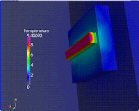
Below are the postprocessing results for the thermal analysis showing the overall package and a close up of the die.
Overall


Die

Elmer has been used for both steady state and transient thermal analysis and has aided greatly in the understanding of the laser thermal performance. I'm a fan of Elmer.

Sunday, July 17, 2011

Sensor Scheme with Ambient Light Correction

In studying estimation methods for control systems I once had a professor say "use all available information". This may seem trivial but it has served as very good advice over many years. In a recent system I have been designing a sensor array to detect light from a display for purposes of calibrating pixel timing versus RBG colors. This method is sensitive to ambient light corrupting the SNR of the signal. However it was observed that the measurement scheme is taking readings in the KHz time span but most ambient light is DC.

As an aside even a florescent bulb is primarily DC ambient luminance. The 60Hz AC mains is applied across a phosphor tube exciting the phosphor to emit light. But due to the persistence the luminance is primarily DC.

The scheme used for correction was to detect when the measurements are not being made. This was readily done by monitoring the control signal to an ADC. When the measurements have been idle for a period defined by a one-shot delay an analog multiplexer circuit integrates the output signal and applies a DC bias to the sensor transimpedance amplifier input. When the output is at zero DC the integrator stops moving and the output stays at zero volts. While a measurement is being made this circuit is opened and the integrator value is held during the measurement time. The result is a sample & hold feedback circuit that dynamically corrects for DC ambient light and prevents saturation of the input stages.

Monday, December 22, 2008

Schottky Diode Thermal Runaway

The problem looked at here is a real-world case of thermal runaway in a Schottky diode. I will use some ideas from closed loop feedback control to analyze the problem. Schottky diodes are used extensively in switching regulators that power nearly every piece of high technology electronics. Putting this in perspective consider the case of a switching supply that converts 5Vdc to -5Vdc in a inverting Cuk topology. Given typical numbers for the output as -5Vdc @ 30ma you might think a Schottky diode rated at 2Amps forward current and 20V reverse breakdown would be perfectly safe. However, Schottky diodes can suffer failure due to thermal runaway caused by excessive reverse current under certain conditions.

The reverse leakage current of a Schottky diode is very sensitive to temperature. In fact it is exponential as follows Ir=I0en·(Tj-To). The power dissipated due to this current is P = Ir·Vrev and the steady-state temperature rise is given to be dT = P·Theta. You can see this is a case of positive feedback. As the temperature rises so does the current. This in turn increases the power dissipation which increases the temperature. This can be analyzed using small signal gain theory applied to the following block diagram.

The small signal loop gain is given by:

g= VrevØ·n·I0en·(Tj-To)

The temperature at which runaway will commence is when the loop gain is greater than unity. Using the small signal gain equation the critical junction temperature is

Tj= T0 + (1/n)·ln(1/(Ø·n·Vrev·Ir0))

As an example consider the MBRM140 diode operating at 60C ambient environment. From the data sheet the maximum leakage Ir(10V,25C)= 0.1mA and Ir(10V,85C)= 10mA . Fitting this data to the exponential results in μ equal to 0.07675. In the inverting -5V application the reverse voltage will be nominally Vrev = 11V. The thermal resistance on the PC board is estimated to be 25C/W. From this data the junction temperature at onset of thermal runaway is Tj= 105.2C. This is a surprisingly low junction temperature that can lead to thermal run away. The reverse voltage is well below specification and the forward current was not even considered in this example. It is a simple exercise to set up an example in an Excel spreadsheet and view the iterations as they evolve.

As noted this analysis included only the reverse leakage current at 100% duty cycle. If there is significant power dissipated in the forward direction that too should be included in the calculation using the appropriate duty cycle. The objective of this note was to show how closed loop control theory can be applied to seemingly non-control problems.

Self-heating Feedback

The basic feedback equation encountered is Gcl = Gf/(1 + Gol) where Gcl is the closed loop gain of a system that has open loop gain Gol and forward loop gain Gf. Consider the case of a resistive heater. The source of power could be either a constant current source or a constant voltage. In this problem we are interested in the steady state temperature of the load.

Constant Voltage Source

For the first case lets look at constant voltage. The power dissipated in the load is P = V2/R. Here R is the load resistance and V is the applied voltage. However, R is a function of temperature, T, given by R = Ro*(1 + a*(T-To) ) where the resistance is linear with temperature and has a value Ro at temperature To. The steady-state temperature is also a function of the temperature given by the dissipation characteristics of the thermal system T = Tamb + theta*P where theta is the thermal resistance (C/W) and Tamb is the ambient temperature. Intuitively you can see that when the voltage is applied the power increases the temperature which in turn increases the resistance (assuming a positive temperature coefficient, a). The increase in resistance then reduces the power. This is inherent negative feedback at play that prevents a runaway thermal condition.
Combining these three equations we can solve for the temperature as

(dT)2 + (1/a)*(dT) - V2*Theta/(a*R0) = 0

Where dT = (T-Tamb). This is a non-linear system. The block diagram is shown below as a feedback network. I also added a thermal time constant to the thermal resistance block. The loop gain is found using small signal gain theory to be -(a*Ro*Theta*I2(dT)) which is negative for a>0.


Constant Current Source

The second case we will look at is a constant current supply. In this case the power dissipation is given by P = I2 * R. We can see intuitively that power dissipation raises the temperature which raises the resistance and therefore increases the power dissipation. This is a case of positive feedback and hence has the potential for thermal runaway. Solving the three equations for power, resistance and temperature we have the result for temperature rise

(T-Tamb) = (I2*R0*Theta) / (1 - (a*Theta*I2*R0))

This is a linear system and has the form of a closed loop equation with open loop gain a*Ro*Theta*I2. In the block diagram below I added a thermal time constant to the thermal resistance block.


Note that for positive temperature coeffficents (a>0) this system has positive feedback. If the loop gain gets too close to unity there will be a thermal runaway condition. Some boundary conditions are: 1. If the temperature coefficient is negative (a<0) dt=I2*R0*Theta, 2. Perfect Heat sink (Theta=0) then dT= 0 and 3. Perfect Short R=0 then dT= 0. The loop gain can be used as a measure of the safety factor in a system design.

This basic analysis of the feedback mechanism in a self heating system has many applications. Who would of thought that a handful of variables would say so much about a system?

Introduction

This is my introduction for this blog. I enjoy engineering design very much; especially describing a problem solution analytically which can then be viewed in the 'real world' as a working mechanism. The link between abstract mathematics and physical reality is fascinating. There is something beautiful in the simplicity of equations. On these pages I plan to periodically post solutions to engineering problems that strike me as interesting. I hope you find it interesting and useful as well. For more information about me visit OmnificSolutions.com


The first topic I plan to write about is how feedback shows up in the equations for thermal heating using a either a constant voltage or current source. An admittedly simple but interesting problem.